
VLSI Solutions & Engineering
frontEnd & BackEnd Verification
Performance-optimized, comprehensive, and cost-effective solutions with shorter time to market
About Us
Providing Excellent Engineering & Design Solutions
Fin Fab Tech is a Hyderabad-based semiconductor design startup delivering high-quality analog layout, physical design, design verification, and analog circuit design services. From past several Years, we have supported customers with reliable layout and verification solutions. Backed by an expert team, we focus on precision engineering, quality, and efficiency to simplify services, accelerate innovation, and enable faster time-to-market.
Partners





Our Services
At Fin Fab Tech, we deliver full-spectrum semiconductor services including Analog layout, physical design, end-to-end design & verification, and analog circuit design—ensuring high-quality, optimized silicon implementation for automotive, and high-performance applications.


Analog Circuit Design
Fin Fab Tech delivers advanced Analog Circuit Design services, covering amplifiers, ADCs/DACs, PLLs, LDOs, bandgap references, comparators, and sensor interfaces used in automotive, AI, IoT, and high-speed communication chips. Our expertise spans low-power, high-speed, and high-accuracy architectures across Bulk CMOS, FD-SOI, and FinFET nodes, following industry best practices to ensure reliable, production-ready silicon comparable to leading semiconductor design service providers.
Analog Layout
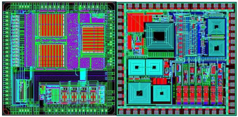
Fin Fab Tech delivers advanced Analog and Mixed‑Signal Layout Design solutions for high‑performance silicon. We support complex designs including ADCs, DACs, SerDes, DDR, PLLs, and image sensor interfaces. Our engineers bring proven tape‑out experience across Bulk CMOS, FD‑SOI, and FinFET technologies. We work confidently from mature nodes to cutting‑edge technologies including 2 nm, 3 nm, and Intel 18A. Our layouts meet first‑silicon goals through rigorous physical verification and sign‑off flows. Fin Fab Tech is a trusted partner enabling quality, speed, and reduced risk to market. service providers.
Design & Verification
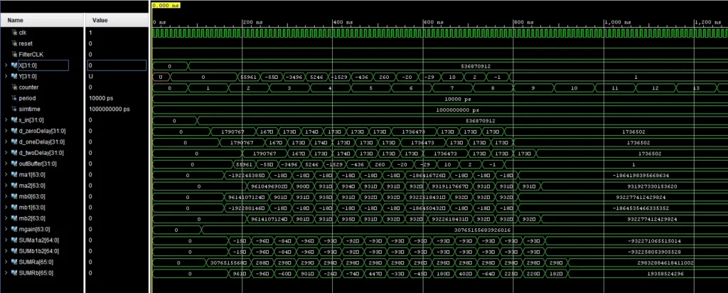
Fin Fab Tech delivers high‑confidence RTL Design Verification services to accelerate silicon success.We help semiconductor teams reduce verification risk, improve quality, and meet aggressive tape‑out schedules.Our senior verification engineers bring 10+ years of proven industry and silicon experience.We specialize in UVM‑based verification using Verilog and SystemVerilog.Our reusable, scalable testbench environments support IP, Subsystem, and SoC‑level verification.We offer deep expertise in critical protocols including AMBA, I2C, I3C, Ethernet, and DDR.Our coverage‑driven approach ensures faster debug, higher coverage closure, and reliable sign‑off.Fin Fab Tech is a trusted verification partner enabling faster time‑to‑market and first‑silicon success.
Physical Design
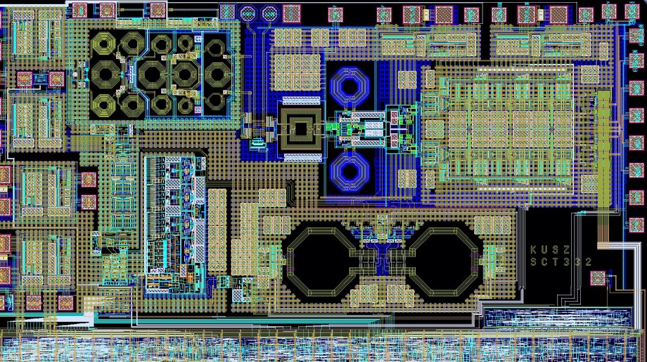
Fin Fab Tech leads the physical design domain, with deep expertise in advanced FinFET technologies at 2nm and 3nm nodes. We deliver end-to-end design solutions, seamlessly driving projects from RTL to GDSII.
Our highly skilled team has hands-on experience with industry‑standard EDA tools across Synopsys, Cadence, and Siemens, enabling us to efficiently support multiple customers across diverse design needs. We specialize in critical sign‑off and analysis areas, including STA, EMIR, DRC, and LVS, ensuring robust, high‑quality silicon deliverables.
Labview Design & Automation
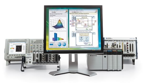
Fin Fab Tech provides advanced LabVIEW Design & Automation services for engineering validation, test automation, and data acquisition systems. We develop modular LabVIEW architectures for hardware-in-loop (HIL), automated test equipment (ATE), signal processing, and control systems. Using NI LabVIEW, PXI, DAQ, and VISA standards, we deliver scalable solutions for semiconductor testing, sensor characterization, and production automation—matching capabilities offered by leading test engineering service providers.
IP Designs
10 BIT ADC
Click ->
Specifications
Technology : TSMC 65 nm
Package Model : Wire Bound Model
Area : 1.5 mm X 2 mm
Frequency : 50 MSPS
12 BIT ADC
Click->
Specifications
Technology : TSMC 65 nm
Package Model : Wire Bound Model
Area : 2 mm X 3 mm
Frequency : 50 MSPS
10 Stage BIT Pipeline ADC
Click->
Specifications
Technology : TSMC 28 nm (HPC+)
Package Model : Flip Chip Model
Area : 3 mm X 3 mm
Frequency : 500 MSPS
12 BIT ADC
Click->
Specifications
Technology : TSMC 65 nm
Package Model : Wire Bound Model
Area : 1 mm X 1 mm
Frequency : 150 MSPS
- Hyderabad
5-3/28/39, Road No.3, Sri sai nagar colony, Boduppal, Hyderabad, Telangana 500092
- Bengaluru
474/2, Sharana Basava Sadana, AECS Layout, B Block, Sigasandra, Kudlu Gate, Bengaluru, Karnataka 560068
- hr@finfabtech.com